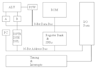
The basic Block Diagram of 8051 Architecture is shown below. The 8-Bit ALU block is linked with the register A, B, SFRs, Register Bank and the I/O ports via 8-Bit Data Bus. The 16-Bit Address Bus is used to link the PC, DPTR, ROM and two I/O port(Higher Address Byte Lower Address Byte).
The addresses of the SFRs of the8051 Architecture.
| Register | Function | Address |
| A | Accumulator | 0x0E0 |
| B | Arithmetic | 0x0F0 |
| DPH | Addressing External Memory | 0x83 |
| DPL | Addressing External Memory | 0x82 |
| IE | Interrupt Enable Control | 0x0A8 |
| IP | Interrupt Priority | 0x0B8 |
| P0 | Port-0 | 0x80 |
| P1 | Port-1 | 0x90 |
| P2 | Port-2 | 0xA0 |
| P3 | Port-3 | 0xB0 |
| PCON | Power Control | 0x87 |
| PSW | Program Status Word | 0x0D0 |
| SCON | Serial Port Control | 0x98 |
| SBUF | Serial Port Data Buffer | 0x99 |
| SP | Stack Pointer | 0x81 |
| TMOD | Timer/Counter Mode Control | 0x89 |
| TCON | Timer/Counter | 0x88 |
| TL0 | Timer-0 Low Byte | 0x8A |
| TH0 | Timer-0 High Byte | 0x8C |
| TL1 | Timer-1 Low Byte | 0x8B |
| TL0 | Timer-0 High Byte | 0x8D |
The General Purpose Registers are divided into four bank Bank-0, Bank-1, Bank-2, and Bank-3. Each bank contains eight number of 8-bit registers. The address starts from 0x00 of first register of Bank-0 to 0x1F address of last register of Bank-3. The 16-Byte of area of Memory is utilized for are bit addressing .The address location starts from the register with address 0x20.
Bank-3
R7 | R6 | R5 | R4 | R3 | R2 | R1 | R0 |
1F | 1E | 1D | 1C | 1B3 | 1A | 19 | 18 |
Bank-2
R7 | R6 | R5 | R4 | R3 | R2 | R1 | R0 |
17 | 16 | 15 | 14 | 13 | 12 | 11 | 10 |
Bank-1
R7 | R6 | R5 | R4 | R3 | R2 | R1 | R0 |
0F | 0E | 0D | 0C | 0B | 0A | 09 | 08 |
Bank-0
R7 | R6 | R5 | R4 | R3 | R2 | R1 | R0 |
07 | 06 | 05 | 04 | 03 | 02 | 01 | 00 |
Bit Addressable Register
Register Address | To Bit Address | From Bit Address |
2F | 7F | 78 |
2E | 77 | 70 |
2D | 6F | 68 |
2C | 67 | 60 |
2B | 5F | 58 |
2A | 57 | 50 |
29 | 4F | 48 |
28 | 47 | 40 |
27 | 3F | 38 |
26 | 37 | 30 |
25 | 2F | 28 |
24 | 27 | 20 |
23 | 1F | 18 |
22 | 17 | 10 |
21 | 0F | 08 |
20 | 07 | 00 |


No comments:
Post a Comment